Analog Circuit
VARIABLE_VOLTAGE_ATTENUATOR
Published:2009/6/18 23:28:00 Author:May | From:SeekIC
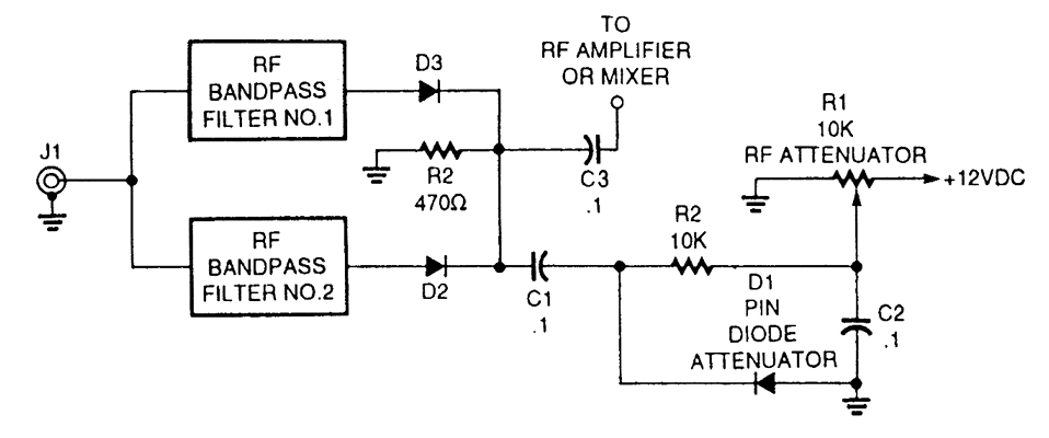
The front-end of this circuit is a bank of selectable bandpass filters. The output of the filter banks are shunted to ground via capacitor (C1) and PIN diode (D1). The PIN diode acts like an electroni-cally variable resistor. The resistance across the diode's terminals is a function of the applied bias voltage. This voltage, hence the degree of attenuation of the RE signal, is proportional to the setting of potentiometer RI. The series resistor (R2) is used to limit the current when the diode is forward biased. This step is necessary because the diode has a very low resistance when a certain rather low potential is exceeded.
Reprinted Url Of This Article:
http://www.seekic.com/circuit_diagram/Basic_Circuit/Analog_Circuit/VARIABLE_VOLTAGE_ATTENUATOR.html
Print this Page | Comments | Reading(3)

Article Categories
power supply circuit
Amplifier Circuit
Basic Circuit
LED and Light Circuit
Sensor Circuit
Signal Processing
Electrical Equipment Circuit
Control Circuit
Remote Control Circuit
A/D-D/A Converter Circuit
Audio Circuit
Measuring and Test Circuit
Communication Circuit
Computer-Related Circuit
555 Circuit
Automotive Circuit
Repairing Circuit
Code: