Basic Circuit
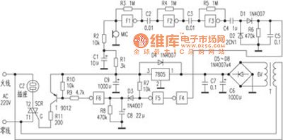
A voice control recording circuit diagram
Published:2014/4/1 21:26:00 Author:lynne | Keyword: A voice control recording circuit diagram | From:SeekIC

When a sound wave compression electret microphone MIC, MIC can output a weak audio signal fed from the NAND gate F1, F2, F3 and R3, R4, R5 constitute the three continuous linear amplification of the amplifier circuit , if consider peak waveform distortion , the output signal amplitude F3 has been large enough , after this signal is coupled through C4 by D1, D2 rectifier get unipolar pulses C5 charging. VC5 soon more than 1/2VDD, the output of NAND gate F4 0, F5 output is 1 , high charge to C8, VC8 also soon be greater than 1/2VDD, F6 output is 0 , the transistor T saturated conduction , SCR is trigger , so 220V mains supply via socket CZ to the recorder , recording starts ; If the sound disappears, the C5 voltage can not be maintained , VC5 quickly dropped to zero. Similarly , C8 only slowly discharge to R8, VC8 about three seconds after the drop to 0 , then , SCR deadline , tape recorders recording aborted ; so, automatic recording control recording ( if necessary delay longer available appropriate to increase the capacity of C8 ) .
This control circuit is not only used for automatic recording recorder can also be extended to other appliances require intermittent voice, interested friends can do it. If the sensitivity is not satisfied, it can be in F1 before adding a transistor amplifier.
Reprinted Url Of This Article:
http://www.seekic.com/circuit_diagram/Basic_Circuit/A_voice_control_recording_circuit_diagram.html
Print this Page | Comments | Reading(3)

Article Categories
power supply circuit
Amplifier Circuit
Basic Circuit
LED and Light Circuit
Sensor Circuit
Signal Processing
Electrical Equipment Circuit
Control Circuit
Remote Control Circuit
A/D-D/A Converter Circuit
Audio Circuit
Measuring and Test Circuit
Communication Circuit
Computer-Related Circuit
555 Circuit
Automotive Circuit
Repairing Circuit
Code: