Index 462
Tianjin VIOS combination instrument circuit diagram(first)
Published:2011/3/29 22:03:00 Author:muriel | Keyword: Tianjin VIOS, combination instrument

Tianjin VIOS combination instrument circuit diagram(first), as shown
Welcome transshipment, the informations are come from Weikue-market net(www.dzsc.com). (View)
View full Circuit Diagram | Comments | Reading(634)
Time delay circuit diagram with monostable trigger CD4528
Published:2011/3/30 2:17:00 Author:muriel | Keyword: Time delay circuit diagram , monostable trigger

Time delay circuit with monostable trigger CD4528
(View)
View full Circuit Diagram | Comments | Reading(2496)
1~99 frequency division(count down) circuit diagram
Published:2011/3/29 21:53:00 Author:muriel | Keyword: 1~99 , frequency division, count down

1~99 frequency division(count down) circuit
(View)
View full Circuit Diagram | Comments | Reading(340)
Time delay circuit diagram of Writing/reading with memory RAM7489
Published:2011/3/30 2:16:00 Author:muriel | Keyword: Time delay circuit diagram , Writing/reading , memory

Time delay circuitwith Writing/reading of memory RAM7489
(View)
View full Circuit Diagram | Comments | Reading(478)
Time delay circuit diagram(first) with comparator 74LS85
Published:2011/3/30 2:16:00 Author:muriel | Keyword: Time delay circuit diagram(first), comparator

Time delay circuit with comparator 74LS85
(View)
View full Circuit Diagram | Comments | Reading(1232)
Time delay circuit diagram(second) with comparator 74LS85
Published:2011/3/30 2:16:00 Author:muriel | Keyword: Time delay circuit diagram(second), comparator

Time delay circuit with comparator 74LS85
(View)
View full Circuit Diagram | Comments | Reading(1648)
Time delay circuit diagram with CC4017 count/distributor
Published:2011/3/30 2:15:00 Author:muriel | Keyword: Time delay circuit diagram, count/distributor

Time delay circuit diagram with CC4017 count/distributor
(View)
View full Circuit Diagram | Comments | Reading(388)
Time delay circuit diagram with 74199 shift register
Published:2011/3/30 2:15:00 Author:muriel | Keyword: Time delay circuit diagram, shift register

Time delay circuit diagram with 74199 shift register
(View)
View full Circuit Diagram | Comments | Reading(1208)
low level signal isolated amplifier circuit diagram with isolated amplifier 3656
Published:2011/3/30 2:15:00 Author:muriel | Keyword: low level signal , isolated amplifier circuit diagram , isolated amplifier

As shown is low level signal isolated amplifier circuit diagram with isolated amplifier 3656:
(View)
View full Circuit Diagram | Comments | Reading(489)
Bipolar V/I isolated converter circuit diagram with isolated amplifier 3656
Published:2011/3/30 2:15:00 Author:muriel | Keyword: Bipolar V/I , isolated, converter circuit diagram, isolated amplifier

As shown is Bipolar V/I isolated converter circuit diagram with isolated amplifier 3656
(View)
View full Circuit Diagram | Comments | Reading(253)
SF1212 automatic exposure integrated(timing) control circuit diagram
Published:2011/3/30 2:14:00 Author:muriel | Keyword: automatic exposure , integrated, timing, control circuit diagram

SF1212 automatic exposure integrated(timing) control circuit (View)
View full Circuit Diagram | Comments | Reading(405)
Power modulator circuit composed of CW7900
Published:2011/3/24 22:05:00 Author:Joan | Keyword: Power modulator
View full Circuit Diagram | Comments | Reading(464)
Capacitive displacement transmitter circuit
Published:2011/3/24 1:30:00 Author:Joan | Keyword: displacement transmitter , Capacitive displacement transmitter

Circuit principle: the multivibrator signal is led out by D2 output. When D2 output is high, the monostable circuit is in a steady state, and D3 output, D4 input, D5 output are low voltage. When D2 output is low, the monostable circuit enters into the temporary stable state. When D3 outputs high voltage, it charges Cx through R3 and RP. Meanwhile, D5 outputs a high level into the U-I output stage, and D4 input voltage decreases exponentially with time. When the voltage is lower than D4 threshold level, the output jumps high, and then jump into a low voltage after being inverted by D5. When the square wave D2 outputted jumps high, Cx is then discharging through R3 and RP until D2 becomes high voltage, which completed a one-shot cycle. Waveform in each point is shown in Figure 2. The output pulse width td is proportional to Cx. The voltage, smoothed by R4 and C2, sent to VT base, is amplified and converted into 4 ~ 20mA DC uniform signal. (View)
View full Circuit Diagram | Comments | Reading(680)
3.3V Voltage output power supply transforming circuit diagram
Published:2011/3/22 22:45:00 Author:Rebekka | Keyword: 3.3V Voltage output, power supply transforming

3.3V Voltage output power supply transforming circuit diagram is shown as below.
(View)
View full Circuit Diagram | Comments | Reading(805)
5V Voltage output power supply transforming circuit diagram
Published:2011/3/22 22:45:00 Author:Rebekka | Keyword: 5V Voltage output, power supply transforming

5V Voltage output power supply transformingcircuit diagram is shown as below.
(View)
View full Circuit Diagram | Comments | Reading(569)
Adjustable output power supply converting circuit diagram
Published:2011/3/22 22:42:00 Author:Rebekka | Keyword: Adjustable output, power supply converting

Adjustable output power supply converting circuit diagram is shown as below.
(View)
View full Circuit Diagram | Comments | Reading(638)
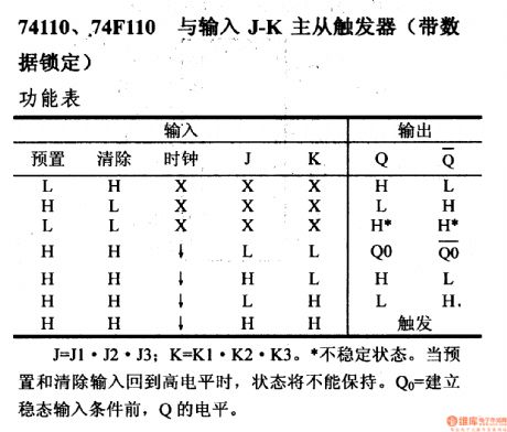
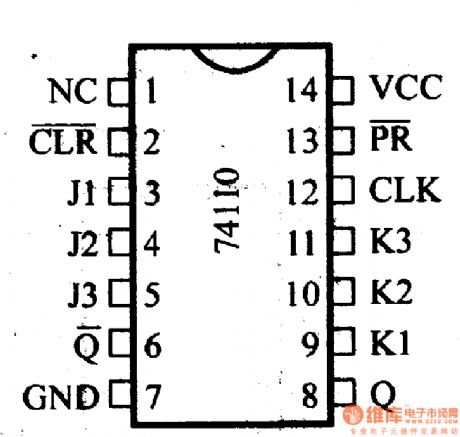
74 series digital circuit of 74110 74F110 input J - K master-slave flip-flop
Published:2011/3/30 2:24:00 Author:Ecco | Keyword: digital circuit, input J - K , master-slave flip-flop


74110 74F110 input J - K master-slave flip-flop(with data caging function)
Unsteady state. When the preset and remove terminal return in high level, the state could not be kept. And the level of Qo is equal to Q before eatablishing steadystate input.
(View)
View full Circuit Diagram | Comments | Reading(463)
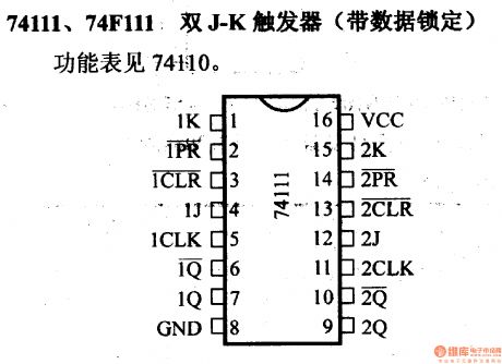
74 series digital circuit of 74111 74F111 double J - K flip-flop
Published:2011/3/30 2:30:00 Author:Ecco | Keyword: digital circuit, double J - K flip-flop

74 series digital circuit of 74111 74F111 double J - K flip-flop(with data caging function)
(View)
View full Circuit Diagram | Comments | Reading(1500)
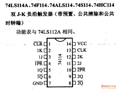
74 series digital circuit of 74LS114A 74F114 double J - K negative edge trigger
Published:2011/3/29 22:38:00 Author:Ecco | Keyword: digital circuit , double J - K negative edge , trigger

74LS114A,74F114, 74ALS114, 74S114, 74HC114double J - K negative edge trigger(with preset, public clear and clock terminal)
(View)
View full Circuit Diagram | Comments | Reading(485)
74 series digital circuit of 74126 74LS126A four buses buffer door
Published:2011/3/29 22:40:00 Author:Ecco | Keyword: digital circuit , four buses buffer door
View full Circuit Diagram | Comments | Reading(1201)
| Pages:462/471 At 20461462463464465466467468469470471 |
Circuit Categories
power supply circuit
Amplifier Circuit
Basic Circuit
LED and Light Circuit
Sensor Circuit
Signal Processing
Electrical Equipment Circuit
Control Circuit
Remote Control Circuit
A/D-D/A Converter Circuit
Audio Circuit
Measuring and Test Circuit
Communication Circuit
Computer-Related Circuit
555 Circuit
Automotive Circuit
Repairing Circuit

