
Index 284
1_kHz_STATE_VARIABLE_BANDPASS
Published:2009/7/2 23:39:00 Author:May

With three 741 opamps or equivalent, circuit gain is Q (reciprocal of damping). Frequency is changed by changing 10K coupling resistors between opamps while keeping their values equal. Increasing resistors 10 times increases frequency 10 times. High-pass output is obtained from first opamp and low pass from second opamp.-D.Lancaster, Active-Filter Cookbook, Howard W. Sams,Indianapolis, IN, 1975, p 156-159. (View)
View full Circuit Diagram | Comments | Reading(561)
200_400_Hz_PASSBAND
Published:2009/7/2 23:39:00 Author:May

Design is based on use of 3.2 for value of Q, to hold passband dip at 1 dB for two-pole filter. Multiple feedback is used for each pole. First opamp can be 741 or equivalent. Centerfrequency is 283 Hz.-D. Lancaster, Active-Filter Cookbook, Howard W.Sams, Indianapolis, IN, 1975, p 166. (View)
View full Circuit Diagram | Comments | Reading(832)
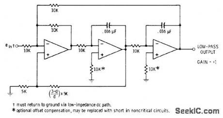
250_Hz_THIRD_ORDER_LOW_PASS
Published:2009/7/2 23:38:00 Author:May

Values shown place cutoff at 250 Hz, with 1-dB dip in response curve. Input must be returned to ground with low-impedance DC path.-D. Lan-caster, Active-Filter Cookbook, Howard W.Sams, Indianapolis, IN, 1975, p 146. (View)
View full Circuit Diagram | Comments | Reading(708)
FM_DEMODULATOR_
Published:2009/7/2 23:28:00 Author:May

Uses Signetics NE564 PLL having postdetection processor, operating from 5-V supply. Conversion gain is low so frequency deviation in input signal should be at Ieast 1%.- Signetics Analog Data Manual, Signetics, Sunnyvale, CA, 1977, p 828-830. (View)
View full Circuit Diagram | Comments | Reading(1568)
BEEPER
Published:2009/7/2 23:24:00 Author:May

Intermittent alarm using 555 timer can be set to energize horn, lights, or other signaling device at any desired interval when tripped. When used on auto, sound cannot be mistaken for stuck horn. Choose SCR rating to handle current drawn by relay and timer. If alarm draws less than 200 mA, relay is not needed.-W. Pinner, Alarm! Alarm! Alarm!, 73 Magazine, Feb. 1976,p 138-139. (View)
View full Circuit Diagram | Comments | Reading(781)
20_2000Hz_VARIABLE_BANDPASS
Published:2009/7/2 23:24:00 Author:May

High-Q active bandpass filter can be adjusted over wide frequency range (100:1) while maintaining Q essentially constant over 100. Two-phase output is available. Opamps can be 741 or equivalent. Cascaded all-pass networks B and C each have 0 to 180° phase variation and unity gain at all frequencies, These are driven by opamp A whose feedback signal is sum of input and output of all-pass networks.R2 adjusts Q,andganged log pots change center frequency,-J.M.worley,Variable Band-Pass Filter, Wireless World,April 1977,p 61. (View)
View full Circuit Diagram | Comments | Reading(972)
1_kHz_THIRD_ORDER_HIGH_PASS
Published:2009/7/2 23:22:00 Author:May

Passband gain is 6 dB for Butter worth filter above 1-kHz cutoff Damping factor is 1.000 for both sections,each using 741 or equivalent opamp,-H.M.Berin, Design of Active Filters,with Experiments, Howard w. Sams, Indianapolis, IN,1977,p 115-116. (View)
View full Circuit Diagram | Comments | Reading(836)
VARIABLE_BANDWIDTH_AF
Published:2009/7/2 23:21:00 Author:May
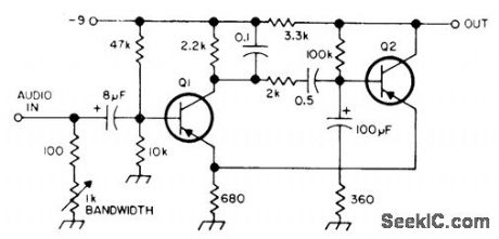
Audio flilter using 1000-Hz Wien bridge provides bandwidths from 70 to 600 Hz Transistors can be SK3004,GE-2,or HEP-254,-Circuits,73 Magazine,Jan,1974,p 124. (View)
View full Circuit Diagram | Comments | Reading(470)
1_kHz_STATE_VARlABLE
Published:2009/7/2 23:20:00 Author:May
Circuit using three 741 opamps offers low sensitivity, voltage-controlled tuning, and easy conversion to high pass or bandpass. For high pass, take output from first opamp. For bandpass, take output from second opamp. To increase frequency, change 10K resistors to identical higher values. 10:1 resistance change produces 10:1 frequency change. Damping d is adjustable; critical value of 1.414 gives maximum flatness of response without overshoot. Design equations are given.-D. Lancaster, Active-Filter Cookbook, Howard W.Sams,Indianapolis, IN, 1975, p129-135. (View)
View full Circuit Diagram | Comments | Reading(519)
TUNING_NULL_INDICATOR
Published:2009/7/2 23:18:00 Author:May

Uses standard left-zero meter as tuning indicator connected in basic opamp AC voltmeter configuration using IC1, with reference buffered by opamp IC2. DC output voltage of tuner is compared with nonzero reference voltage; as these voltages approach each other during tuning, meter pointer moves toward zero, and abruptly reverses direction as tuning null point is passed. Diode D1, protects meter from overload. Use any lowleakage diodes for bridge.-A. S. Holden, Sensitive Null Indicator, Wireless World, Oct. 1974, p 381. (View)
View full Circuit Diagram | Comments | Reading(1327)
1_kHz_BIQUAD_BANDPASS
Published:2009/7/2 23:18:00 Author:May

Three 741 opamps are connected to give two integrators and inverter. Overall gain is -Q, determined by value of input resistor used. Circuit is tuned by varying capacitors in steps. Absolute bandwidth remains constant asfrequency changes. Chief applications are in telephone systems, where identical absolute-bandwidth channels are required.-D. Lancaster, Active-Filter Cookbook, Howard W. Sams, Indianapolis, IN, 1975, p 159-164. (View)
View full Circuit Diagram | Comments | Reading(727)
1_kHz_THIRD_ORDER_LOW_PASS
Published:2009/7/2 23:17:00 Author:May

Circuit using 741 or equivalent opamp consists of unity-gain first-order section followed by equal-component voltage-controlled voltage-source secondorder section.-H. M. Berlin, Design of Active Filters, with Experiments, Howard W. Sams, Indianapolis, IN, 1977, p 113-114. (View)
View full Circuit Diagram | Comments | Reading(770)
VOLTAGE_TUNED_STATE_VARIABLE
Published:2009/7/2 23:16:00 Author:May


Provides choice of high-pass, bandpass, and low-pass outputs, each with cutoff frequency variable between 1 and 6 kHz by varying control voltage between -10 V and +15 V,Output load resistor sets voltage gain between input and output. Gain-control input varies gain from maximum set by load resistor down to zero.Input signals must be limited to 100 mV because input circuit is differential amplifier operating without feedback.-D. Lancaster, Active-Filter Cookbook, Howard W. Sams, Indianapolis, IN, 1975, p 203-205. (View)
View full Circuit Diagram | Comments | Reading(730)
320_Hz_LOW_PASS
Published:2009/7/2 23:14:00 Author:May

Frequency dependent negative-resistance circuit uses 747 dual opamp, Signal source used as input should have low resistance, and load should have high resistance. Voltage-follower stages can be used to isolate both input and output of filter.-R.Melen and H. Garland, Understanding IC Operational Amplifiers, Howard W. Sams, Indianapolis, IN, 2nd Ed.,1978, p 104-105. (View)
View full Circuit Diagram | Comments | Reading(573)
2_W_2_METER_PHASE_LOCKED_FM_TRANSMIT_TER
Published:2009/7/2 23:13:00 Author:May
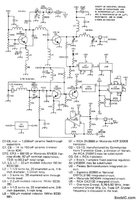
Operating frequency of 144-148 MHz is generated directly, without using frequencymultiplier stages. Oscillator stability is achieved by phase-Iocking oscillator to crystal. Tuning range of 143-149 MHz corresponds to varactor control voltage of 1-4 V, which maintains proper loop gain across entire band, ECL decade divider U2 is Plessey SP647 driving Schottkyclamped divider U3B to give overall division of 50. Phase detector and Ioop amplifier functions are in U4. Pierce crystal oscillator Q3 feeds buffer Q4 interface with TTL levels. Microphone preamp U5 is slightly overdriven so speech waveform is clipped or Iimited. With phaseIocked circuit, frequency stability is as good as that of crystal used in reference oscillator. Divide desired operating frequency by 25 to get crystal frequency.-A. D. Helfrick, A Phase-Locked 2-Meter FM Transmitter, QST, March 1977, p 37-39, (View)
View full Circuit Diagram | Comments | Reading(856)
LATCHING_PROBE
Published:2009/7/2 23:12:00 Author:May
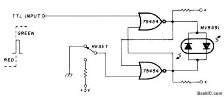
TTL pulse catcher can be used as logic probe for IC troubleshooting. Uses Monsanto MV5491 dual red/green LED, with 220 ohms in upper lead to +5 V supply and 100 ohms in lower +5 V lead because red and green LEDs in parallel back-to-back have different voltage requirements. SN75454 driver circuit is cross-coupled to form latch or memory element. Positive-going pulse sets latch and makes LED change color to indicate arrival of pulse. Latch must be reset manually with RESET switch. Also useful for locating intermittents such as glitches; probe can be left connected to circuit under test, to see if latch hasbeen set by unwanted signaL-K. Powell, Novel Indicator Circuit, Ham Radio, April 1977, p 60-63. (View)
View full Circuit Diagram | Comments | Reading(716)
TEST_PROBE
Published:2009/7/2 23:06:00 Author:May
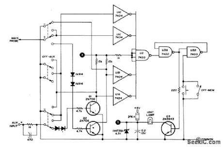
Checks binary levels and pulse coincidence. Indicator lamp, driven by switching transistor 03, is bright enough to be seen in sunlight. Close OFF-MEM switch when using probe as binary level indicator, to eliminate need for pushing button continuously. At AUX position of main switch, two inputs are needed at same time. To check for coincidence, connect patch cord from AUX jackto second point being checked in logic circuit. All signal diodes are 1N914. Probe drain is about 160 mA; changing to LED would cut drain to 6O mA.-R. H. Fransen, Improved Logic Test Probe, Ham Radio, Dec. 1973, p 53-55. (View)
View full Circuit Diagram | Comments | Reading(590)
AUDIBLE_PROBE
Published:2009/7/2 23:00:00 Author:May
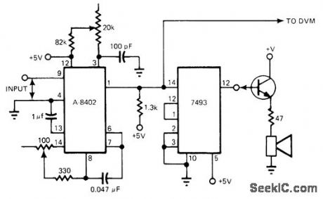
Speeds troubleshooting by eliminating need to look at meter, and prevents possible damage to logic under test by minimizing possibility of shorts occurring if probe slips when looking at meter. Components used with A-8402 IC give 1-kHz output for 6-V input.Binary counter divides this signal to give output in low audio range and converts to square wave more suitable for driving loudspeaker. Probe can also serve as input for digital voltmeter.When probing TTL circuits, probe gives low frequency for 0 state, high frequency for 1, and middle frequency for open circuit. Output transistor type is not criticaL-G. E, Row, Audible Logic Probe Doubles as DVM Input Section, EDNMagazine, Oct. 20, 1977, p 82. (View)
View full Circuit Diagram | Comments | Reading(481)
SINGLE_LED_TUNING_INDICATOR
Published:2009/7/2 22:58:00 Author:May
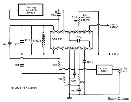
Circuit shown, when driven by IF output of FM tuner, permits tuning for maximum brightness of single LED such as 50824403. Article gives choice of two tuning indicator circuit awangements that can be used with the SBA750 limiting IF amplifier and detector IC. Recommended version of tuning indicator uses Plessey SL3046 five-transistor array with discrete resistors and capacitor to drive LED. Arrangement gives very clear, sensitive indication of correct tuning point to within a few millivolts.-J. A. Skingley, Sensitive F.M. Tuning Indicator, Wireless World, June 1974, p 173-174. (View)
View full Circuit Diagram | Comments | Reading(1312)
HIGH_SPEED_HALF_WAVE_RECTIFIER
Published:2009/7/2 22:57:00 Author:May
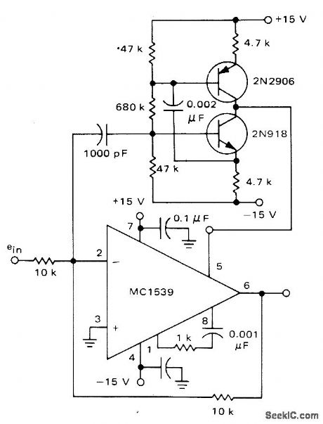
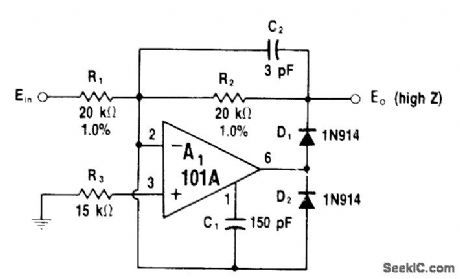
Produces inverted haff-wave replica of input signal with Iow error at frequencies up to 100 kHz. C1 provides feed-forward compensation. For negative-going output. reverse connections to diodes.-W. G. Jung. IC Op-Amp Cookbook. Howard W. Sams. Indianapolis. IN. 1974. p 191-192 (View)
View full Circuit Diagram | Comments | Reading(672)
| Pages:284/471 At 20281282283284285286287288289290291292293294295296297298299300Under 20 |
Circuit Categories
power supply circuit
Amplifier Circuit
Basic Circuit
LED and Light Circuit
Sensor Circuit
Signal Processing
Electrical Equipment Circuit
Control Circuit
Remote Control Circuit
A/D-D/A Converter Circuit
Audio Circuit
Measuring and Test Circuit
Communication Circuit
Computer-Related Circuit
555 Circuit
Automotive Circuit
Repairing Circuit