Other Circuit
Multi-Stage Output Delay Circuit
Published:2011/7/27 8:41:00 Author:Robert | Keyword: Multi-Stage, Output, Delay | From:SeekIC
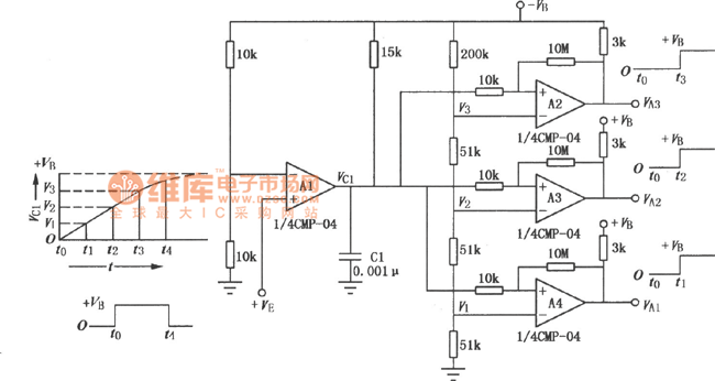
The picture shows the multi-stage output delay circuit. In the circuit it uses the operational amplifier as the comparator. When the operational amplifier A1's in-phase input port is added the +VE voltage, the voltage VC1 on the operational amplifier A2, A3, A4's in-phase input ports would increase by following the law of exponential curve. The operational amplifier's out-phase input port is added the voltage provided by the voltage classification divider. So each operational amplifier's input would reverse each output signal separately at the time of t1, t2, t3 during Vc1 is from zero to +VB(power voltage). That achieves the purpose of VA1, VA2, VA3's delaying progressively. It should be noted that this circuit uses dual power supplies which is positive power +VE, +VB and negative power -VB.
Reprinted Url Of This Article:
http://www.seekic.com/circuit_diagram/Amplifier_Circuit/Other_circuit/Multi_Stage_Output_Delay_Circuit.html
Print this Page | Comments | Reading(3)

Article Categories
power supply circuit
Amplifier Circuit
Basic Circuit
LED and Light Circuit
Sensor Circuit
Signal Processing
Electrical Equipment Circuit
Control Circuit
Remote Control Circuit
A/D-D/A Converter Circuit
Audio Circuit
Measuring and Test Circuit
Communication Circuit
Computer-Related Circuit
555 Circuit
Automotive Circuit
Repairing Circuit
Code: