Other Circuit
Gain Programmable Amplification Circuit Composed Of OPA676
Published:2011/8/4 20:52:00 Author:Robert | Keyword: Gain, Programmable, Amplification | From:SeekIC


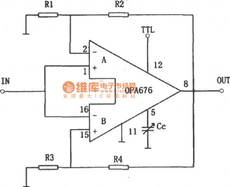
The picture shows the gain programmable amplification circuit. This circuit is mainly made up of OPA676 integrated chip. And the OPA676's internal part has two channels amplification circuit which is marked as A channel and B channel separately (see the A and B in the picture). The two channels' conducting mode or not conducting mode are controlled by the pin 12's voltage level (which is called TTL port). If the TTL port's voltage is high level, the A channel (the higher part of the circuit) would work and the B channel (the lower part of the circuit ) would be not conducted. Otherwise when the TTL port is in low voltage level, the A channel would be not conducted and the B channel would work. The A channel's voltage magnification is AVA=1+R4/R3, and the B channel's voltage magnification is AVB=1+R4/R3. So it could only select different R1, R2 or R3, R4, the A and B channels would have different gain. By controlling the A and B channels selection port TTL's voltage level (pin 12), it could be easy to achieve the gain programmable control.
Reprinted Url Of This Article:
http://www.seekic.com/circuit_diagram/Amplifier_Circuit/Other_circuit/Gain_Programmable_Amplification_Circuit_Composed_Of_OPA676.html
Print this Page | Comments | Reading(3)

Article Categories
power supply circuit
Amplifier Circuit
Basic Circuit
LED and Light Circuit
Sensor Circuit
Signal Processing
Electrical Equipment Circuit
Control Circuit
Remote Control Circuit
A/D-D/A Converter Circuit
Audio Circuit
Measuring and Test Circuit
Communication Circuit
Computer-Related Circuit
555 Circuit
Automotive Circuit
Repairing Circuit
Code: