Amplifier Circuit
1880MHz Inside Collector Biased Amplifier Composed Of RF2324 Application Circuit
Published:2011/10/23 21:44:00 Author:May | Keyword: 1880MHz, Inside Collector Biased Amplifier | From:SeekIC
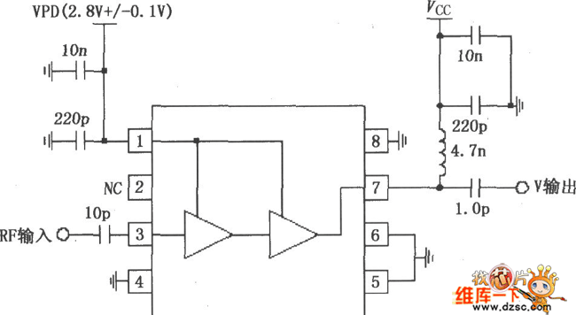
RF signals (RF) is input by pin 3 and output by pin 7 after enlarging by pre-amplifier and power amplifier. Pin 3 is directly coupled with internal amplifier. So, it adds a 10pF blocking coupling capacitor. The matching impedance is 50Ω when it works at 1880MHz. Pin 7 is output end of collector, whichcan connect power supply Vcc through choke or matching inductance. The typical matching impedance of this pin is 50Ω. In order to get the largest output power and efficiency, it connects to matching network outside to make the output impedance of amplifier match with it. Pin 1 is power down controlling end. The circuitworks when VPD=2.8V±0.1V (typical value of IPD is 8.5mA) and is closed when VPD<0.9V. VFD needs to add RF bypass circuit.
Reprinted Url Of This Article:
http://www.seekic.com/circuit_diagram/Amplifier_Circuit/1880MHz_Inside_Collector_Biased_Amplifier_Composed_Of_RF2324_Application_Circuit.html
Print this Page | Comments | Reading(3)

Article Categories
power supply circuit
Amplifier Circuit
Basic Circuit
LED and Light Circuit
Sensor Circuit
Signal Processing
Electrical Equipment Circuit
Control Circuit
Remote Control Circuit
A/D-D/A Converter Circuit
Audio Circuit
Measuring and Test Circuit
Communication Circuit
Computer-Related Circuit
555 Circuit
Automotive Circuit
Repairing Circuit
Code: