
Project Solutions
HIGH-END POWER AMP-High-class watts (3)
Published:2011/8/21 21:02:00 Author:Phyllis From:SeekIC
By Ton Giesbets
To protect the loudspeakers against output offset voltage transients that may occur when the mains voltage is switched on, a switch-on delay is provided for the output relay. The delay time is approximately 6-7 seconds. The state of the relay depends on the supply voltage for the final amplifier, rather than the transformer voltage. If the supply voltage drops below 17 V, MOSFET T18 de-energizes the relay.
The MOSFET starts to conduct when its gate voltage is approximately 2.5 V. The threshold value can vary from one FET to the next, so the delay time can also vary. The gate is connected directly to the supply voltage via voltage divider R42-R44. Diode D12 prevents C18 from holding the MOSFET in the ’on’ state when the supply voltage drops, and D13 ensures that CIS discharges if the supply voltage drops below half its normal value. This avoids excessive reduction in the delay time if the amplifier is switched on too quickly after being switched off.
The relay coil is connected to the supply voltage via R45, so a relay with a lower coil voltage can be used by changing the value of R45. Be sure to use a resistor with an adequate power rating.
The DC protection circuit is also coupled to the switch-on delay circuit. It de-energizes the relay by quickly discharging C18 in the switch-on delay circuit. If a positive DC voltage is present, T16 will conduct and discharge capacitor C18 via R40 if the voltage at the amplifier output is greater than +1.5 V If an excessively large negative voltage is present at the output, T17 will conduct due to the negative voltage on its emitter. In this case, the discharge current from C18 must flow through R37 and R38. The resistance value of voltage divider R42-R44 also determines the values of R37-R39. The latter values must be kept relatively low, since otherwise the threshold for detecting a negative DC voltage on the amplifier output would be too great. It is approximately -3.5 V with 100-kfl resistors. This means that the circuit is somewhat less sensitive to negative DC voltages than to positive DC voltages, but that does not have any practical consequences.
Overdrive indicator
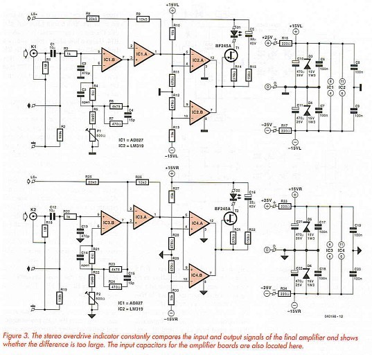
As the output power of this amplifier is rather modest by contemporary standards, it’s quite possible for it to be overdriven during loud music passages, which will result in clipping. For this reason, a reliable LED indicator circuit has been added to the design to indicate overdrive conditions. The indicator circuit (Figure 3) constantly compares the output signal with the input signal and generates a warning if they do not match. Apart from having greater amplitude, the output signal from the amplifier should have the same phase and frequency characteristics as the input signal. 
The signals are compared by attenuating the output signal and amplifying the input signal. The input signal amplifier built around IClb (or IC3b for the other channel, which is not further described here) simulates the transfer characteristics of the final amplifier as well as possible using simple means. For instance, RC network R3/C2 has approximately the same time constant as the low-pass filter at the input of the final amplifier (R1//R2 and CI). R3 and C4 are reserved for unusual input configurations in other applications and are not used here. The network formed by C4 and R7 does not have much effect here, but it is included for the sake of completeness.
Reprinted Url Of This Article: http://www.seekic.com/blog/project_solutions/2011/08/21/HIGH_END_POWER_AMP_High_class_watts_(3).html
Print this Page | Comments | Reading(1346)
Article Categories
New published articles
· Imagination works with TSMC to develop FinFET process
Author:Ecco Reading(33897)
· XMOS pushes event-driven MCUs with lower price
Author:Ecco Reading(3538)
· Intel brings upgraded 32-nm SoC for smartphones
Author:Ecco Reading(3255)
· Micron pushes TLC 128-Gbit NAND flash
Author:Ecco Reading(3854)
· Intel will stop supplying desktop motherboards
Author:Ecco Reading(5350)
· Processor market was expected to regain strength in 2013
Author:Ecco Reading(3323)
· It was reported that TSMC sales fall steeply
Author:Ecco Reading(3480)
· Cisco, NXP work with auto wireless startup
Author:Ecco Reading(3625)
· Micron was impacted by manufacturing glitch
Author:Ecco Reading(4021)
· China can make 22-nm transistor by themselves
Author:Ecco Reading(3828)
· Chip market rebound is coming, according to survey
Author:Ecco Reading(3766)
· Sony, Toshiba will spend more on chips, iSuppli reports
Author:Ecco Reading(3794)
· Qualcomm becomes the 13th company to join NFC Forum board
Author:Ecco Reading(6109)
· TSMC increases building work for FinFET fab
Author:Ecco Reading(3781)
· TI plans to cut 1,700 jobs in OMAP shift
Author:Ecco Reading(4623)