
Project Solutions
Rolling Dice (2)
Published:2011/8/2 21:37:00 Author:Phyllis From:SeekIC
By Paul Goossens
Main PCB
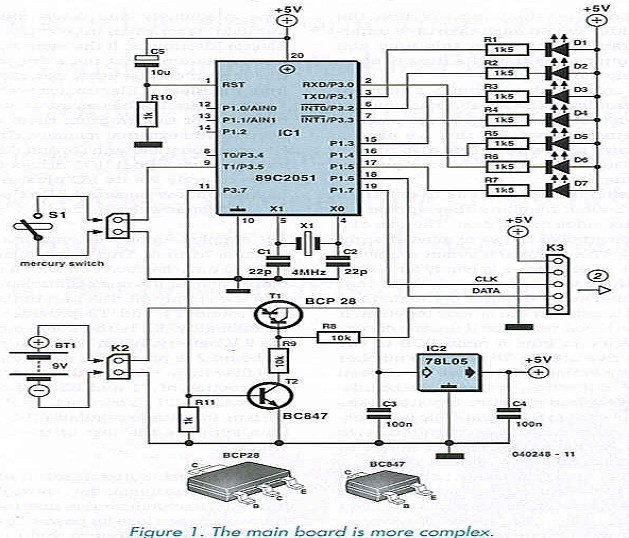
After these considerations we arrived at the circuits for the dice. At the hart of the circuit is IC1, a microcontroller by Atmel (Figure 1). We have used this type previously and have given a detailed description in past issues of Elektor Electronics. It therefore suffices just to mention that the software for this project can be freely downloaded from the Elektor Electronics website. As this controller has an internal flash memory for the program there is no need to add external memory. Crystal XI in conjunction with C2 and CI provide a clock signal. IC1 drives the 7 LEDs directly via its I/O pins. As we have used low-current LEDs there is no need for an extra buffer. 
The supply section may appear a little unusual at first. This is because we want to turn the circuit on with a pushbutton and let the microcontroller itself turn the supply off. The part of the circuit round Tl and T2 provides this functionality. K2 is the connector for the 9 V battery. When push-button SI on board 2 is pressed, a small current will flow from + 9 V via the base/emitter junction of Tl and R8 to ground. This causes Tl to conduct, feeding a current to voltage regulator IC2. This then supplies the rest of the circuit with 5 V.
When the push-button is released, the current can no longer flow through R8. It is of course undesirable that the circuit would then lose its power. Just try to keep the push-button held down during a throw; it’s not exactly user-friendly for a dice.
To get round this problem we’ve added resistor R9 and transistor T2. T2 is driven via the microcontroller. When the circuit is switched on, T2 is also turned on, causing a current to flow from the base of Tl to ground via R9 and T2. The supply is then no longer dependent on SI being pressed.
When the processor notices that it hasn’t moved for a while (several minutes), it stops driving T2. The dice then turns itself off automatically. When switch SI is pressed again, the whole sequence repeats itself.
When the supply is applied a reliable reset signal is generated for the microcontroller by C5 and R10.
The CLK and DATA signals are fed to the next board via connector K3. K3 also has connections for the supply and the on-switch (pin 5). The switch had to placed on board 2 due to a lack of room on the main board.
Other boards
The circuits for the other boards (2 to 6) are almost identical. The main difference is that circuit 2 has a switch, which isn’t present on the other boards. 
Figure 2 shows the circuit diagrams for board 2 and the other four boards. There is obviously no need for a feed-through connector (K2) on the last board.
At the centre of the circuit is the shift register, a 74HCT4094. This type of IC has a parallel output register. Every rising edge at the clock input causes the 8 bit data in the IC to shift by one bit. The first bit then takes the value of the data input. The last bit shifted out is connected via pin 9 to the data input of the shift register on the following board. This effectively turns all boards into one large shift register.
Reprinted Url Of This Article: http://www.seekic.com/blog/project_solutions/2011/08/02/Rolling_Dice__(2).html
Print this Page | Comments | Reading(901)
Article Categories
New published articles
· Imagination works with TSMC to develop FinFET process
Author:Ecco Reading(33516)
· XMOS pushes event-driven MCUs with lower price
Author:Ecco Reading(3534)
· Intel brings upgraded 32-nm SoC for smartphones
Author:Ecco Reading(3250)
· Micron pushes TLC 128-Gbit NAND flash
Author:Ecco Reading(3816)
· Intel will stop supplying desktop motherboards
Author:Ecco Reading(5341)
· Processor market was expected to regain strength in 2013
Author:Ecco Reading(3318)
· It was reported that TSMC sales fall steeply
Author:Ecco Reading(3474)
· Cisco, NXP work with auto wireless startup
Author:Ecco Reading(3620)
· Micron was impacted by manufacturing glitch
Author:Ecco Reading(4017)
· China can make 22-nm transistor by themselves
Author:Ecco Reading(3819)
· Chip market rebound is coming, according to survey
Author:Ecco Reading(3760)
· Sony, Toshiba will spend more on chips, iSuppli reports
Author:Ecco Reading(3790)
· Qualcomm becomes the 13th company to join NFC Forum board
Author:Ecco Reading(6103)
· TSMC increases building work for FinFET fab
Author:Ecco Reading(3778)
· TI plans to cut 1,700 jobs in OMAP shift
Author:Ecco Reading(4587)