
Project Solutions
Drop-in Microcontroller Board (3)
Published:2011/7/27 21:39:00 Author:Phyllis From:SeekIC
Building it
Having purchased the printed circuit board and all components you are ready to start building the circuit. As shown in Figure 4, the PCB consists of two sections that are easily separated using a hacksaw. One section is for the interface with the PC, the other, for the drop-in module proper. 
In view of the relatively small number of parts, building up the two sub-boards is unlikely to take much of your time. As usual, we recommend you start with the low-profile parts. For the rest, hardly anything that can go wrong if you stick to the component overlay on the PCB and, of course, the parts list.
Connectors K1-K5 have to be soldered at the underside of the board, their task being to link the module to the host equipment in which is to function. Figure 5 shows our ready-assembled and tested board. 
Before we can test the circuit, we need to look at the software.
Software
The galaxy of features offered by the PSD813F1 may startle instead of encourage. A chip with so many functions is usually difficult to configure and you may quickly feel lost in bits and bytes. Fortunately, STMicroelectronics have written a clearly structured program called PSD-soft Express that may be obtained free of charge from their website at www.st.com. The documentation with the PSD813 series is impressive to say the least.
The program comes with a wizard guiding you through the configuration process in a step-by-step manner, using unambiguous questions. You’ll quickly get the hang of the program simply by using it a few times.
To enable everyone to make a head start with the PSD813 chip we produced a small example program that may be downloaded free of charge from our website. The program demonstrates how extra ChipSelect signals and I/O ports may be generated and created respectively.
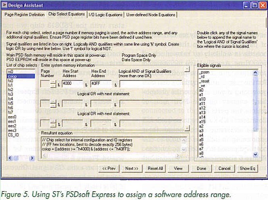
Having launched PSDSoft Express you are ready to create a new project. Programming the PSD chip could not be easier using the wizard. The individual pins of the PSD chip connected to the JTAG interface and the controller are immediately assigned names by the wizard. Figure 6 illustrates the ease of defining an extra CS signal. Once all steps have been completed, the PSD chip is ready for programming through the JTAG interface. 
Finally
The PSD831 chip offers far more possibilities than those used in our simple example. None the less, the drop-in module discussed in this article will not fail to underline the versatility and multifunctional character of the PSD813xxx chips. Together with a suitable microcontroller, these chips form a solid base for a wide range of applications. The PSD813xxx allows much space to be saved in circuits normally requiring an EPROM, Flash memory and a handful of discrete logic.
Thanks to the extensive software support and the ability to be programmed through a JTAG interface, the chip will easily prove worth its salt during circuit development and debugging. Updates to the chip software and hardware (in the CPLD parts) are also easy to implement using the same JTAG interface.
Reprinted Url Of This Article: http://www.seekic.com/blog/project_solutions/2011/07/27/Drop_in_Microcontroller_Board__(3).html
Print this Page | Comments | Reading(450)
Article Categories
New published articles
· Imagination works with TSMC to develop FinFET process
Author:Ecco Reading(33527)
· XMOS pushes event-driven MCUs with lower price
Author:Ecco Reading(3534)
· Intel brings upgraded 32-nm SoC for smartphones
Author:Ecco Reading(3250)
· Micron pushes TLC 128-Gbit NAND flash
Author:Ecco Reading(3816)
· Intel will stop supplying desktop motherboards
Author:Ecco Reading(5341)
· Processor market was expected to regain strength in 2013
Author:Ecco Reading(3318)
· It was reported that TSMC sales fall steeply
Author:Ecco Reading(3474)
· Cisco, NXP work with auto wireless startup
Author:Ecco Reading(3620)
· Micron was impacted by manufacturing glitch
Author:Ecco Reading(4017)
· China can make 22-nm transistor by themselves
Author:Ecco Reading(3820)
· Chip market rebound is coming, according to survey
Author:Ecco Reading(3761)
· Sony, Toshiba will spend more on chips, iSuppli reports
Author:Ecco Reading(3790)
· Qualcomm becomes the 13th company to join NFC Forum board
Author:Ecco Reading(6105)
· TSMC increases building work for FinFET fab
Author:Ecco Reading(3778)
· TI plans to cut 1,700 jobs in OMAP shift
Author:Ecco Reading(4587)