
Project Solutions
Hands-on CPLDs -Part I: Experimental rev counter (3)
Published:2011/7/20 22:10:00 Author:Li xiao na From:SeekIC
By A. Rosenkranzer
The peripheral circuitry

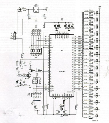
Figure 2 shows the detail circuit diagram of the tachometer. IC1 is the CPLD type EPM7128S from Altera packaged in a 84-pin PLCC outline. The chip has a total of eight ground pins that must all be connected to GND.
There are also two types of VCC connection on the chip. Two of these connections (both called VCCINT) are connected to the core of the chip while the other six (VCCIO) supply power to the I/O buffers. This supply can be connected to either 3.3 V or as in our case 5 V. For other applications it would be useful to be able to use 3.3 V if it was found necessary to reduce the EMI produced when the buffers switch or it would greatly simplify interfacing to 3.3 V logic.
For supply decoupling it is good practice to use at least one 100 nF capacitor for each VCC connection sited as close as possible to the pin and one or two tantalum capacitors (10 to 22 jiF) to reduce any supply rail noise.
Four connections are used for the JTAG programming interface (TDI, TMS, TDO and TCK). TCK is the clock input used during programming. TDI is not as you may have thought some kind of diesel engine but in this case the data input signal. This signal together with the data output (TDO) allows several CPLDs to be daisy chained by connecting TDO to TDI of the next chip. The TDO of the last chip is then connected to the JTAG interface. TMS is used to configure the JTAG interface for reset, data, command, boundary scan and so on. All four pins are fitted with a 10 k£2 pull-up resistor.
The connector for the JTAG-Interface (K2) is a 10-way header plug. Along with the four signal wires are also ground and VCC to supply power to the programming adaptor (ByteBlaster). The four JTAG connections can also be used as general-purpose I/O pins but this is only advisable if there are no other I/O pins available.
Rl and C12 provide a reset pulse to the active low Global CLeaR input (GCLRn) during power-up. This reset clears all the chips internal registers.
GCLK1 is the first of the two global clock inputs. It is important to ensure that the first system clock for the CPLD is connected to this input and not to some general purpose I/O pin which is not internally wired to the cells and registers. Two I/O pins close to the GCLK1 input are used as a buffer to interface to the crystal. The output from the buffer is connected directly to GCLK1 input. Resistor R22 reduces the output loading while the 100 K£2 resistor R21 in parallel to the crystal provides a positive feedback path for the buffer.
Pin OE1 is a general Output Enable, and must be defined in the programming data. OE2 (GCLK2) is another special function pin and can be used as either a second clock input (for designs with two clocks) or as a second output enable input. In the tachometer design described here both of these functions are not required.
All other components and external signals are connected to general-purpose I/O pins. The criteria used to allocate these pins will be explained in the follow-up article in Elektor Electronics.
Reprinted Url Of This Article: http://www.seekic.com/blog/project_solutions/2011/07/20/Hands_on_CIPtLGJs:The_peripheral_circuitry.html
Print this Page | Comments | Reading(1369)
Article Categories
New published articles
· Imagination works with TSMC to develop FinFET process
Author:Ecco Reading(33527)
· XMOS pushes event-driven MCUs with lower price
Author:Ecco Reading(3534)
· Intel brings upgraded 32-nm SoC for smartphones
Author:Ecco Reading(3250)
· Micron pushes TLC 128-Gbit NAND flash
Author:Ecco Reading(3816)
· Intel will stop supplying desktop motherboards
Author:Ecco Reading(5341)
· Processor market was expected to regain strength in 2013
Author:Ecco Reading(3318)
· It was reported that TSMC sales fall steeply
Author:Ecco Reading(3474)
· Cisco, NXP work with auto wireless startup
Author:Ecco Reading(3620)
· Micron was impacted by manufacturing glitch
Author:Ecco Reading(4017)
· China can make 22-nm transistor by themselves
Author:Ecco Reading(3820)
· Chip market rebound is coming, according to survey
Author:Ecco Reading(3761)
· Sony, Toshiba will spend more on chips, iSuppli reports
Author:Ecco Reading(3790)
· Qualcomm becomes the 13th company to join NFC Forum board
Author:Ecco Reading(6105)
· TSMC increases building work for FinFET fab
Author:Ecco Reading(3778)
· TI plans to cut 1,700 jobs in OMAP shift
Author:Ecco Reading(4587)