

Industry News
UBM starts teardown analysis of Intel Ivy Bridge CPU
Published:2012/4/12 2:57:00 Author:Ecco From:SeekIC
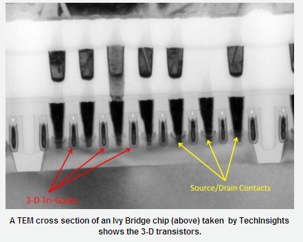
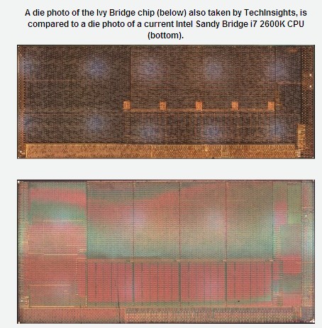
UBM TechInsights announced that they would start a teardown analysis of an Intel Ivy Bridge processor. However, UBM TechInsights has an Ivy Bridge processor marked as a 3.3GHz Core i5-3550 chip which is packaged in Malaysia. It has a die size of 170 mm2, down from 208 mm2 for the current Sandy Bridge i7 2600K CPU. The Ivy Bridge chips are the first to use Intel’s 22 nm process technology with 3-D transistors.
According to most of the semiconductor industry, the next big process is a 28 nm technology. Altera and Xilinx have already made 28 nm FPGAs, AMD and Qualcomm. They are making 28 nm chips in the process at foundries including GlobalFoundries and TSMC.
Intel’s 22 nm technology is unique with 3-D transistors otherwise known as FinFETs. The transistor designs should be in lower power leakage. In any case, other chip makers will develop similar technologies in sub 20 nm processes.
UBM TechInsights aims to deliver two reports based on its examination of the Ivy Bridge chip. It will release a logic detail structural analysis report covering the chip’s process technology, logic cells, embedded memory, logic and I/O transistors with high res images of the chip and its key regions.
In its initial tests, UBM TechInsights found gate pitches of 90nm in the embedded SRAM array in the processor. It also found logic regions with gate lengths of 22 nm.
Reprinted Url Of This Article: http://www.seekic.com/blog/IndustryNews/2012/04/12/UBM_starts_teardown_analysis_of_Intel_Ivy_Bridge_CPU.html
Print this Page | Comments | Reading(1241)
Article Categories
New published articles
· Imagination works with TSMC to develop FinFET process
Author:Ecco Reading(33479)
· XMOS pushes event-driven MCUs with lower price
Author:Ecco Reading(3534)
· Intel brings upgraded 32-nm SoC for smartphones
Author:Ecco Reading(3250)
· Micron pushes TLC 128-Gbit NAND flash
Author:Ecco Reading(3816)
· Intel will stop supplying desktop motherboards
Author:Ecco Reading(5341)
· Processor market was expected to regain strength in 2013
Author:Ecco Reading(3318)
· It was reported that TSMC sales fall steeply
Author:Ecco Reading(3474)
· Cisco, NXP work with auto wireless startup
Author:Ecco Reading(3620)
· Micron was impacted by manufacturing glitch
Author:Ecco Reading(4017)
· China can make 22-nm transistor by themselves
Author:Ecco Reading(3819)
· Chip market rebound is coming, according to survey
Author:Ecco Reading(3759)
· Sony, Toshiba will spend more on chips, iSuppli reports
Author:Ecco Reading(3789)
· Qualcomm becomes the 13th company to join NFC Forum board
Author:Ecco Reading(6103)
· TSMC increases building work for FinFET fab
Author:Ecco Reading(3778)
· TI plans to cut 1,700 jobs in OMAP shift
Author:Ecco Reading(4587)